
Industry
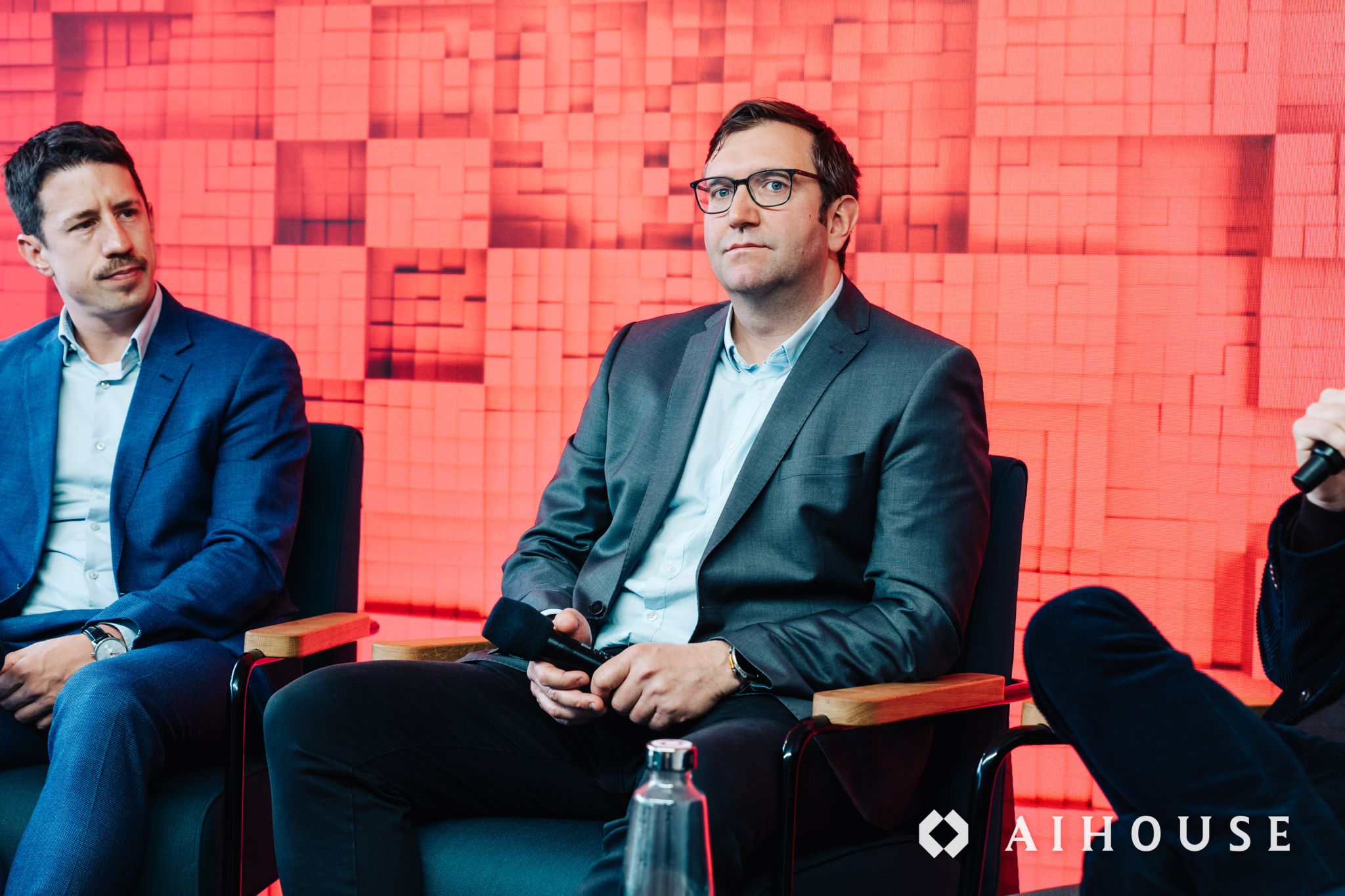
Chipmind CEO Harald Kröll talking about AI-based Chip Design at AI House at the WEF 2026 in Davos
January 20, 2026
1 min read
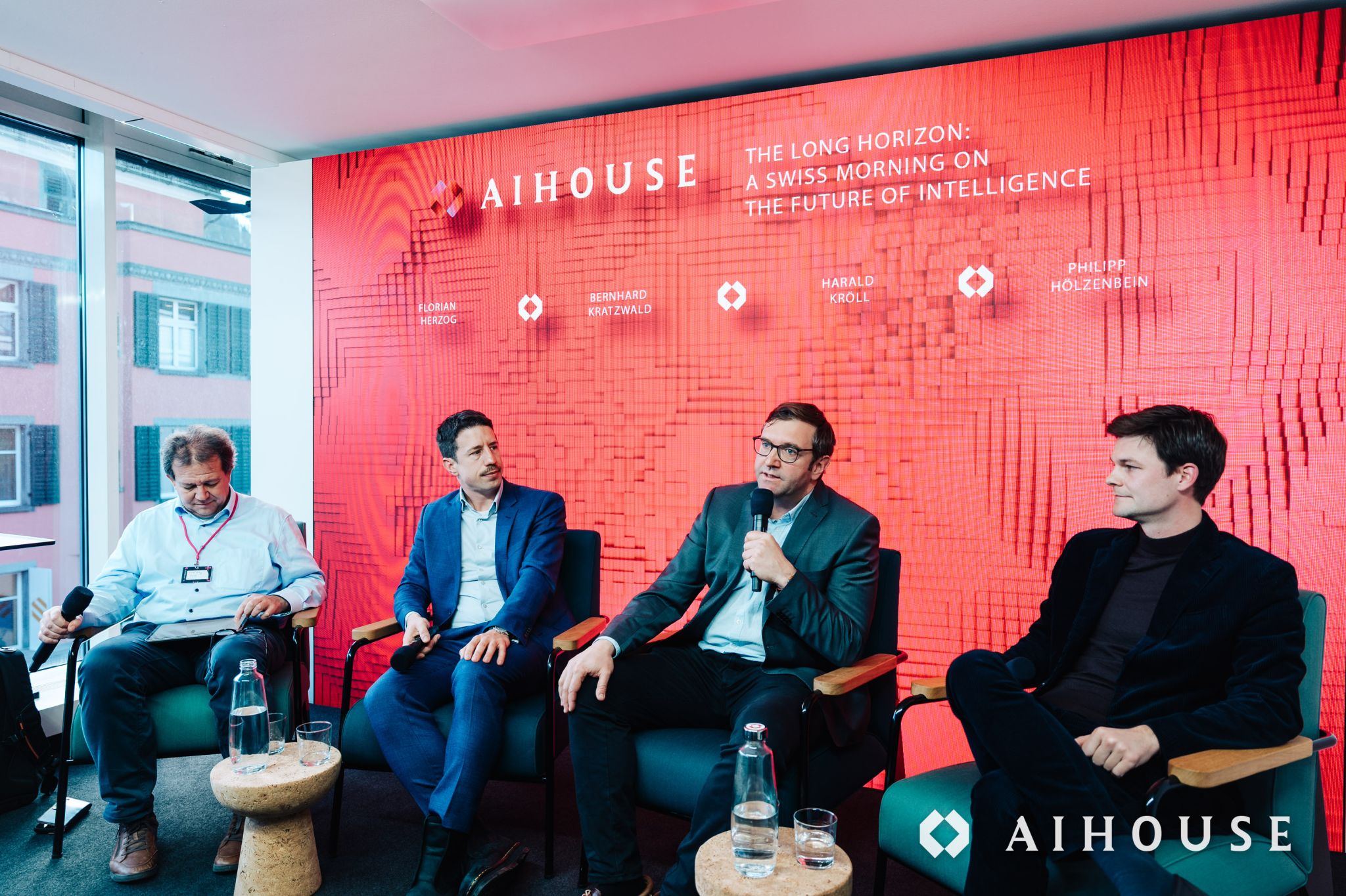
In many companies, LLM endpoints provide intelligence like electricity at the top. But the actual work often needs to get done in development flows and environments at the bottom. This "gap area" for chip design is the natural habitat of the Chipminds — where we live and thrive 🐿️.
Sandro Belfanti and I enjoyed our time at AI House Davos alongside the World Economic Forum (WEF) annual meeting, where I joined the panel last week, where I joined the panel "GenAI is More Than LLMs" to discuss this shift.
Bridging the Workflow Gap
While general models offer broad capabilities, true acceleration in the semiconductor industry happens when AI is natively woven into complex EDA and development environments. Moving beyond standard LLMs means building design-aware systems engineered specifically for hardware workflows.
Special thanks to my fellow panelists for a fantastic discussion:
Together, we are shaping how autonomous intelligence reshapes the future of digital chip design.

Ready to see Chipmind in action? Book a Call.
Backed by & Featured in







Let AI do the chips.